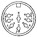
Signal pin No. |
Signal Name |
Signal |
Beschreibung |
1 |
GND |
- |
Signal Ground |
2 |
TXD |
Out |
Transmitted data |
3 |
RXD |
In |
Received data |
4 |
RTS |
Out |
Request to send |
5 |
CTS |
In |
Clear to send |
6 |
DSR |
In |
Data set ready |
7 |
DTR |
Out |
Data terminal ready |
8 |
CD |
In |
Carrier detect |
E |
FG |
- |
Protective Ground |
Serial Interface (Floppydisk Port)

Signal pin No. |
Signal Name |
Signal |
Beschreibung |
1 |
GND |
- |
Signal Ground |
2 |
PTX |
Out |
Transmitted data |
3 |
PRX |
In |
Received data |
4 |
POUT |
In |
Transmit mode |
5 |
PIN |
Out |
Receive mode |
E |
FG |
- |
Protective ground |
System-Bus
Pin |
Symb |
Bedeutung |
1 |
VB |
Stromversorgung von Batterie 1,0A unreg. |
2 |
-NMI |
Active LOW |
3 |
V |
(geschaltet) 50mA |
4 |
+5V |
(geschaltet) |
5 |
DB7 |
Data Bit 7 |
6 |
DB6 |
" |
7 |
DB5 |
" |
8 |
DB4 |
" |
9 |
DB3 |
" |
10 |
DB2 |
" |
11 |
DB1 |
" |
12 |
DB0 |
Data Bit 0 |
13 |
-IOCS |
Adresse 0000-007F I/O Chip select |
14 |
VC |
Power for RAM 40mA |
15 |
AB0 |
Adress Bus |
16 |
AB1 |
" |
" |
" |
" |
30 |
AB15 |
" |
31 |
-Reset |
CPU Reset , active low |
32 |
-R/W |
Memory read (low) write (high) |
33 |
-Reset |
RAM Protect bei Power off |
34 |
E |
von CPU Clock |
35 |
ROM EN |
low, disable ROM |
36 |
-EXT INT |
External interupt |
37 |
GND |
Ground |
38 |
GND |
Ground |
39 |
CG |
Case Ground |
40 |
CG |
Case Ground |
![]() zurück
zurück